 EnglishEnglish


| Size: | |
|---|---|
| Orientation: | |
| Quantity: | |


JSD
INFI
untra-thin CVD diamond film for thermal conductivity 49*60*0.96
1.High wear resistance to chipping and fracture
2.Excellent thermal stability
3.Excellent toughness sharpness
4.Various size
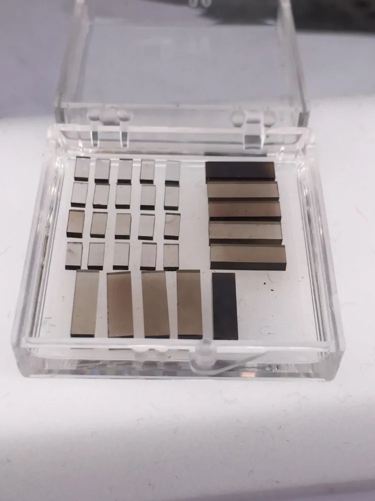
Polycrystalline CVD diamond
polycrystalline CVD (chemical vapour deposition) synthetic diamond products are manufactured by a chemical vapour deposition (CVD) process and are subject to tightly controlled growth conditions during manufacturing and equally stringent quality control procedures.
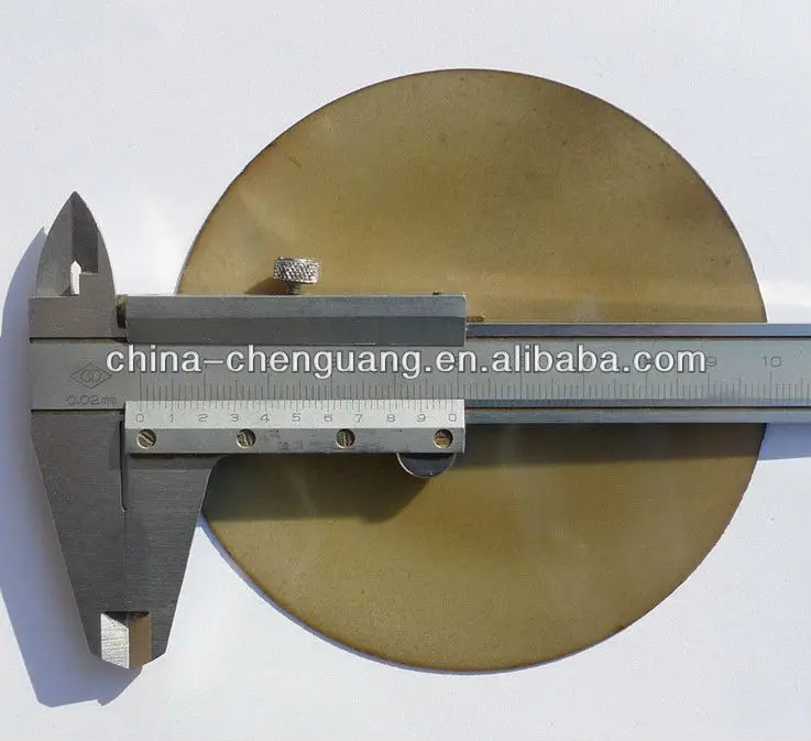
untra-thin CVD diamond film for thermal conductivity 49*60*0.96
1.High wear resistance to chipping and fracture
2.Excellent thermal stability
3.Excellent toughness sharpness
4.Various size
Polycrystalline CVD diamond
polycrystalline CVD (chemical vapour deposition) synthetic diamond products are manufactured by a chemical vapour deposition (CVD) process and are subject to tightly controlled growth conditions during manufacturing and equally stringent quality control procedures.


